Last visit was: Sat Jul 19, 2025 12:24 am
|
It is currently Sat Jul 19, 2025 12:24 am
|
a simple cpu 20 bits wide
| Author |
Message |
|
oldben
Joined: Mon Oct 07, 2019 2:41 am
Posts: 814

|
I am now working on the ALU schematic and thinking of the PCB for it.
Some changes have been made for ALU with the CTL schematic.
Trial PCB layout will 9.5 inches x 7.5 inches.
The FPGA version for ALTERA DE1 (cyclone II) now stable and the programming
file for the cpu is avaible.
You do not have the required permissions to view the files attached to this post.
|
| Sat Feb 29, 2020 6:31 pm |
|
|
|
oldben
Joined: Mon Oct 07, 2019 2:41 am
Posts: 814
|
Fighting the system here, with Ki-Cad. Ball park is looking at 9 x 9 inch cards.
The main two schematics are drafted, the alu (36 TTL) and the control section (25 ttl). The front panel card is the other main section, with memory and I/O and the mother board,straight forward
logic. Memory is 16KB per card, with 32KB for user program/data and 12KB ram/prom for the OS.
Serial IO and a SD card emulating 2 8 inch floppies. 4.9 Mhz clock and a 6809 style memory cycle.
You do not have the required permissions to view the files attached to this post.
|
| Mon Mar 02, 2020 11:10 pm |
|
|
|
roelh
Joined: Mon Oct 07, 2019 1:26 pm
Posts: 50
|
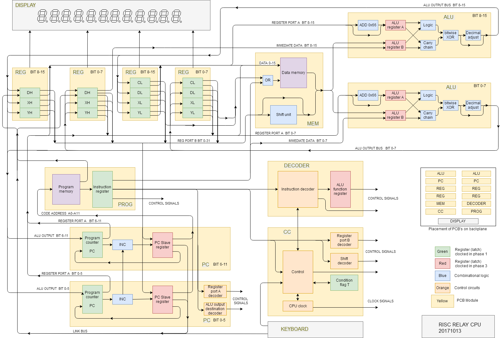
Hi Ben, I'm trying to understand your design. I am missing a high-level block diagram and description. Since there are two LS170 I suppose there are 8 registers. And also, a clear description of the instruction word. At the beginning of the thread you did some ASCII diagrams but for me that is not sufficient to understand all. It is difficult to reverse-engineer the design from your schematic. Especially the control section that mostly has gates and labels. For ascii drawings I suggest http://asciiflow.com/. Another great online tool for diagrams is draw.io I used that for my relay computer: https://cdn.hackaday.io/images/4603351507992625211.pngWhy do you use counters as instruction register ? Is there a reason for using obsolete components, I suppose you still have a lot of them laying around ? The LS170 could be replaced by HC670 (tristate) that is still available. Your design goals are similar to my Kobold K2 (8 registers, 16 bit data, 18/20 bit address). Kobold is a lot simpler though, because it has no microcode. See https://hackaday.io/project/167605-kobold-k2-risc-ttl-computer.
Last edited by BigEd on Tue Mar 03, 2020 7:29 pm, edited 1 time in total.
fix link
|
| Tue Mar 03, 2020 8:17 am |
|
|
|
oldben
Joined: Mon Oct 07, 2019 2:41 am
Posts: 814
|
Quote: Hi Ben, I'm trying to understand your design. I am missing a high-level block diagram and description. Since there are two LS170 I suppose there are 8 registers. And also, a clear description of the instruction word. At the beginning of the thread you did some ASCII diagrams but for me that is not sufficient to understand all. It is difficult to reverse-engineer the design from your schematic. Especially the control section that mostly has gates and labels. For ascii drawings I suggest http://asciiflow.com/. Another great online tool for diagrams is draw.io I used that for my relay computer: https://cdn.hackaday.io/images/4603351507992625211.pngThe design of this computer was set to be the early 1970's, around the time of the PDP-8/e, with small PROMS just coming out. The basic design was 18 bits with 9 bit bytes. 4 registers PC,AC,IX,SP and simple indexing. Later revision moved the design to A,B,X,S and PC, thus two 74LS170's. Quote: Why do you use counters as instruction register ?
I needed a loadable register, with clear. Quote: Is there a reason for using obsolete components, I suppose you still have a lot of them laying around ? The LS170 could be replaced by HC670 (tristate) that is still available.
74170 is a 1970's part. The microcode is simple rom look up tables, load from fetch, and bump state counter. The goal was good general puropse computer with index and stack. The Alu data path is simple, 18 bits data in bus, 18 bits data out. Ram and alu in the middle. Memory cards latch data out for address and data. The complex part is 9/18 bit data, a bit messy with byte i/o chips. The front panel makes use of data out, on a instruction fetch on some instructions to display information. Still a work in progress until draft out some PCB's. Thank you for the url's.
Last edited by BigEd on Tue Mar 03, 2020 9:15 pm, edited 2 times in total.
fix quoting tags
|
| Tue Mar 03, 2020 8:57 pm |
|
|
|
roelh
Joined: Mon Oct 07, 2019 1:26 pm
Posts: 50
|
Thank you for your explanation. I now understand that you want to build a computer that could have been build in the 1970's.
Good luck with design and construction, I will follow it !
|
| Tue Mar 03, 2020 9:11 pm |
|
|
|
oldben
Joined: Mon Oct 07, 2019 2:41 am
Posts: 814
|
I have expanded the 18 bit computer, to 20 bits on the DE1.
This required new connectors 23x2 for the TTL version.The control section is now down to 23 chips. The alu section has expanded to 46 chips.
Bytes are 10 bits. Words 20 bits. Load,store,and,or,eqv,add,sub,adc,sbc binary logic.
Adx,Axc are excess three decmal addition, normal and add with carry.
This gives a me a Octal Computer (~7 digits) that has the feel of computing from
the Cretaceous era, or before C ~ 1971..1973 with core memory and early MSI TTL.
This version is LS TTL version, from about 1976-1977 with MOS ram interfacing, but
same instruction set as the core memory version. A SDC card provides 2 drives of 255 K,
10 bit bytes. Serial is 2400 baud. No IRQ is used by the I/O devices. Most of the development
now will be software (rom) libraries for decmial and long arithmitic (40 bits).
You do not have the required permissions to view the files attached to this post.
|
| Sat Mar 07, 2020 6:36 am |
|
|
|
BigEd
Joined: Wed Jan 09, 2013 6:54 pm
Posts: 1836
|
I'd be interested to hear more about the SD card interface- is there any software layer or a microcontroller?
|
| Sat Mar 07, 2020 2:17 pm |
|
|
|
oldben
Joined: Mon Oct 07, 2019 2:41 am
Posts: 814
|
A simple 8 bit shift reg in hardware and BIOS routines for reading/writing 512 x 10 bit sectors. This site was very usefull for SD details: http://elm-chan.org/cc_e.htmlLater I will use Sparkfun SD breakout PCB for a 74X breadboarded prototype off the DE1 expanson connectors. FPGA routing race conditions tends to delay DE1 development for days when the hardware config fails to work for that unlucky day.
|
| Sat Mar 07, 2020 10:42 pm |
|
|
|
oldben
Joined: Mon Oct 07, 2019 2:41 am
Posts: 814
|
Now working on version #2
You do not have the required permissions to view the files attached to this post.
|
| Sun Mar 15, 2020 12:23 am |
|
|
|
oldben
Joined: Mon Oct 07, 2019 2:41 am
Posts: 814
|
I had to shufflle opcode encoding around to get LEA (load effective Address)to work
with Y registor. S and Z(ero) page are now word addressing only. Encodng is a bit messy
as it adds a few more gates to encode register operands.
|
| Tue Mar 17, 2020 4:42 am |
|
|
|
oldben
Joined: Mon Oct 07, 2019 2:41 am
Posts: 814
|
The hardware and software have reached a stable state, and considered version #1.
Development is halted as I am moving to bigger things like 32 bits.
|
| Sun Mar 22, 2020 7:52 pm |
|
Who is online |
Users browsing this forum: Applebot, claudebot, PetalBot, SemrushBot and 0 guests |
|
You cannot post new topics in this forum
You cannot reply to topics in this forum
You cannot edit your posts in this forum
You cannot delete your posts in this forum
You cannot post attachments in this forum
|
|