.
Some interesting information about the 68020, from 1984.
First,
a blog post with some patent references:
Quote:
The Motorola MC68020 holds a special place in my heart because it was used in the Amiga 1200, which was the first computer I owned which was a pleasure to use and program.
Next, some stats from
a 1988 book about the device, by Werner Hilf and Anton Nausch, also Motorola employees:
Quote:
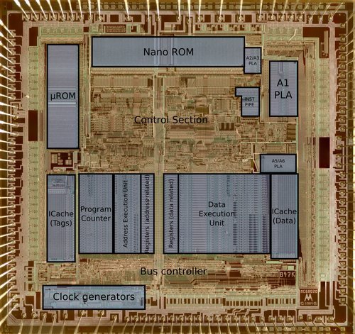
68000 had 68,000 transistors, chip size 6.2 by 7.1mm.
68020 had 200,000 transistors, chip size 7.1 by 7.1mm.
2¼ micron HCMOS-III technology, 5ns propagation delay per logic gate.
Drawings for the chip layout were 150 square meters in total.
Schematics were 46 square meters in total.
Test software for the chip had half a million lines of code.
A "prototype" was built from 300 MSI (medium scale integration) chips on 14 PCBs.
-
M68000 Familie Teil 2 Anwendung und Bausteine (translated freely from
the German text.)
There's also a detailed 1984 paper
The Motorola MC68020 by Doug MacGregor, Dave Mothersole, and Bill Moyer, all of Motorola, which gives slightly different numbers - possibly an earlier revision in a less advanced technology:
Quote:
The MC68020 is 9.22 mm on a side. lt was designed with an HCMOS technology to minimize power consumption (it consumes 1 to 1.5 watts) and allows for high clock frequencies (16 MHz, for the worst case). lt utilizes about 190,000 transistors, 103,000 of which are actually implemented.
What's an unimplemented transistor? Most likely it means they've counted every transistor site in the ROMs and PLAs, where on average only half would be present, depending on programming.
Quote:
The primary design goals of the MC68020 were compatibility and performance. The chip's performance was significantly increased through the use of many different techniques-parallelisrl, pipelining, increased clock frequency, increased bus width, special-purpose units, new instructions and addressing modes, and an instruction cache.
Quote:
Increased clock frequency. One of the simplest ways to increase performance is to increase the clock frequency at which a part executes. The MC68000 and its derivative, the MC68010, have a frequency range of 8 MHz to 12.5 MHz. On the MC68020, the base frequency has been increased to 16 MHz, and it is is not unreasonable to expect 20 MHz or above in the future.
Quote:
It is now possible to build a machine that is very fast internally, but that machine must still communicate with the external world. Thus it is important to minimize the delay due to executing bus cycles. This is done by reducing the minimum bus cycle time from four clock cycles to three clock cycles, and by reducing the number of bus cycles to be excuted by providing a 32-bit data bus and a256-byte instruction cache. The instruction cache reduces the execution time in two ways. First, it provides a two-clock-cycle access time for an access that hits in the cache, and second, if the access hits in the cache, it allows simultaneous instruction and data accesses to occur. Of these two benefits, simultaneous instruction and data access is more significant since it allows a 100 percent reduction in the time required to access the instruction rather than the 33 percent reduction afforded by going from three clocks to two clocks. Reducing cache access time further (below two clocks) would not be beneficial, since the time required to update the instruction stream pointers would be two clocks as well.
Lots more interesting reading in that paper, and several interesting tables and diagrams too. Notably the 68020 also extends the instruction set: there's an example of an array access, which takes 79 clocks on the 68000, 50 clocks running the same code on a 68020, and just 32 clocks using the new addressing mode.