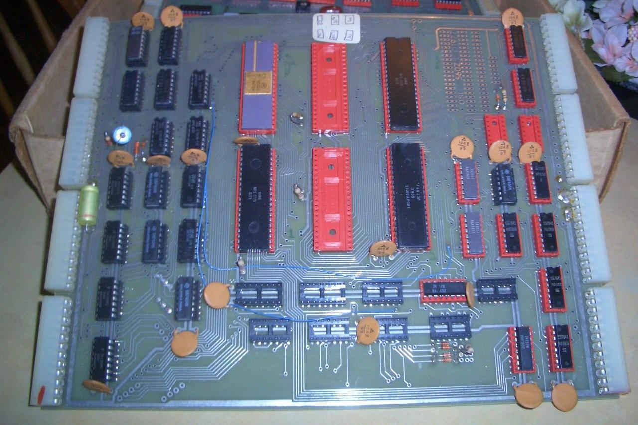
View unanswered posts | View active topics It is currently Thu Mar 28, 2024 3:13 pm


Reply to topic  [ 3 posts ] 
 Ohio Scientific's 560Z board - Z80 and PDP-8E 
Author Message

Joined: Wed Jan 09, 2013 6:54 pm
Posts: 1780
Here's an oddity: a back-end processor board to be used with a 6502 front-end, with Z80 and PDP-8E capability. You'll need further boards for the RAM, one for each 4k you need.

See http://osi.marks-lab.com/boards/boards.html
Quote:
Supports Z80 CPU and IM-600 (PDP-8 compatible) microprocessors plus three-way bus switching and run/single step circuitry. The 560Z runs under the command of a 6502 based 400, 500, or 510 system. Can support 64K of memory & I/O, but occupies only 4K of 6502 memory through a "sliding port-hole"

Image

Manual: http://www.osiweb.org/manuals/OSI560Z.pdf
Schematics: http://osi.marks-lab.com/boards/schematics/OSI560Z.pdf


Wed Jun 11, 2014 9:04 am
Profile
User avatar

Joined: Tue Jan 15, 2013 5:43 am
Posts: 189
Gosh, that is an oddity! BTW there's a typo; I'm sure they mean 6100 (made by Harris and Intersil), not 600. But it's a twelve-bit CPU! And apparently it and the Z80 are under control of the 6502 host system.

http://en.wikipedia.org/wiki/Intersil_6100

I took a peek at the linked page, and was startled at what a wide variety of boards OSI offered. Here's a combo board, featuring a 6800, a 6502 and a Z80. Just the thing for an enthusiast from the 1970s who wants to cover all the bases (or can't make up his mind)!

-- Jeff


Attachments:
OSI510.jpg
OSI510.jpg [ 232.4 KiB | Viewed 4347 times ]

_________________
http://LaughtonElectronics.com
Sun Jun 15, 2014 1:08 am
Profile WWW

Joined: Tue Dec 11, 2012 8:03 am
Posts: 285
Location: California
PCB technology from back then amazes me with its primitiveness. We used a board house in 1992 that could make 0.002"-wide traces on multilayer boards, but 10 years before that was another story, like the picture above. I remember Computer Design magazine around 1988 or 89 advertising VME boards with wall-to-wall thru-hole ICs such that you couldn't see the board except at the edge (or of course the back). The first commercial PCB layout I did was only three years before that, and I was told to not go below .025" trace width. That was when we drew it out on velum, 2X or 4X actual size, then put the film over it and taped it up with the crepe tape and the patterns from Bishop Graphics. Then we drove the films to the graphic-arts house to get them reduced to something the board house could use, then picked them up and took them to the board house. First article was very expensive compared to today. The first time someone told me about CAD and sending files over the modem in 1986 or 87, it seemed like a different world. The 1980's seemed to bring the quickest advances in PCB manufacturing ability.

_________________
http://WilsonMinesCo.com/ lots of 6502 resources


Sun Jun 15, 2014 2:55 am
Profile WWW
Display posts from previous:  Sort by  
Reply to topic   [ 3 posts ] 

Who is online

Users browsing this forum: No registered users and 6 guests


You cannot post new topics in this forum
You cannot reply to topics in this forum
You cannot edit your posts in this forum
You cannot delete your posts in this forum
You cannot post attachments in this forum

Search for:
Jump to:  
cron
Powered by phpBB® Forum Software © phpBB Group
Designed by ST Software