EPiC - A new 68k multi-processor motherboard project
| Author |
Message |
|
Garth
Joined: Tue Dec 11, 2012 8:03 am
Posts: 285
Location: California

|
Size, and the resulting lengths of connections, is heavily involved. The smaller you can make it, the better behaved it will be for a particular method. However, note that you will also be able to make the board smaller with four layers than with two. That will also affect the price of the board, reducing the price difference between two- and four-layer. I have not conferred with Jeff to be able to speak for him, but I'll expand on the jumper idea, with something he might have had in mind. On rare occasion, cost and other constraints have forced me to cut into the ground plane to put a jumper in it. I make the cut absolutely as small as I can, because the return current for those traces going over the jumpers has to go around the hole, negatively impacting the AC behavior. This picture gives the idea, on a tiny 2-layer RF PCB where I did not have the room for zero-ohm resistors: Attachment:
 GndPlaneJmp.jpg [ 11.18 KiB | Viewed 8351 times ]
The dark green is the back-side copper. Trace and space are .006". (I apologize for the poor picture quality. I'll skip the boring explanation.) mercury0x000d wrote: According to this, a four layer board contains power and ground planes. So one would connect the grounds from all components into the ground plane (along with any connections which need permanently grounded or logic low-ed) and hook all the positive supply lines (along with any connections which need to permanent be logically high) to the power plane and then the routing of all the signal carrying traces (address and data buses and chip enable / control lines) gets done on the outer top and bottom layers, correct? Yes. The ground plane is the most important. If you absolutely have to have a third signal layer to get things routed in a reasonable amount of space, you can route the power as traces instead of a plane, then put bypass capacitors from each power-supply pin to the ground plane absolutely as close to that pin as possible. Quote: Speaking of the dev board's two layers, what are your thoughts on me making the component side double as a ground plane and run power and signals on the solder side? If you use SMT, the signal side will have to be the component side, while the ground is the back. With thru-hole, you'll probably want the signals on the back, so you can do some cut-and-jumper corrections if necessary after the parts are soldered on. _________________http://WilsonMinesCo.com/ lots of 6502 resources
|
| Wed Jul 23, 2014 8:41 pm |
 
|
|
|
mercury0x000d
Joined: Tue Jun 03, 2014 2:40 pm
Posts: 127
|
Garth wrote: ...
Yes. The ground plane is the most important. If you absolutely have to have a third signal layer to get things routed in a reasonable amount of space, you can route the power as traces instead of a plane, then put bypass capacitors from each power-supply pin to the ground plane absolutely as close to that pin as possible.
... You mean if I use both a power and a ground plane I don't have to use bypass caps on anything? On a side note, I need to start over on my schematic. Fritzing apparently has a bug in its trace routing when there's hundreds of traces. That'll teach me to use beta-level software. -_-
|
| Wed Jul 23, 2014 11:01 pm |
|
|
|
Garth
Joined: Tue Dec 11, 2012 8:03 am
Posts: 285
Location: California
|
mercury0x000d wrote: You mean if I use both a power and a ground plane I don't have to use bypass caps on anything? I believe I read that there's no inductance in the power and ground connections in the board itself if you have the two parallel planes, meaning you would not need bypass capacitors at each IC. That's for infinite planes, but you can appoximate that closely enough by keeping connections and transmission lines away from the edge by at least a few times as much as the thickness of the dielectric, which with four evenly spaced layer in .062"-thick board is about .020". I have not been able to find it again though, as I look through Dr. Howard Johnson's articles. Quote: On a side note, I need to start over on my schematic. Fritzing apparently has a bug in its trace routing when there's hundreds of traces. That'll teach me to use beta-level software. -_- If you're talking about an autorouter, I would encourage not depending on one much. If/when you use one, you will probably need to do a manual inspection and clean-up afterward, possibly fixing a few problems and routing a few things that it might not have been able to. If you can take the time to do it by hand though, you can get better density and better high-frequency behavior. _________________http://WilsonMinesCo.com/ lots of 6502 resources
|
| Thu Jul 24, 2014 1:30 am |
|
|
|
mercury0x000d
Joined: Tue Jun 03, 2014 2:40 pm
Posts: 127
|
Garth wrote: ...
If you're talking about an autorouter, I would encourage not depending on one much. If/when you use one, you will probably need to do a manual inspection and clean-up afterward, possibly fixing a few problems and routing a few things that it might not have been able to. If you can take the time to do it by hand though, you can get better density and better high-frequency behavior. No, I did every single trace by hand. Multiple times, if you count all the revisions I did while I was still deciding what the best layout would be. Oh well.
|
| Thu Jul 24, 2014 4:14 am |
|
|
|
Garth
Joined: Tue Dec 11, 2012 8:03 am
Posts: 285
Location: California
|
So was it a bug in the ratsnesting? Or other problem?
_________________http://WilsonMinesCo.com/ lots of 6502 resources
|
| Thu Jul 24, 2014 4:34 am |
|
|
|
mercury0x000d
Joined: Tue Jun 03, 2014 2:40 pm
Posts: 127
|
Garth wrote: So was it a bug in the ratsnesting? Or other problem? Basically, yeah. It appears you have your traces all laid out, then you go to modify a wire and suddenly it morphs into something resembling spaghetti, connections disappearing at random points one moment then reappearing differently the next so that you have to delete the entire wire segment and redo it. This can be done, and the problem (usually) doesn't come back, at least on that line, however any little screw-up with my traces discredits the software in my mind. I don't want there to be some hidden, software-induced design error in my PCB that I only catch after it's fabbed and under power. Much easier to rebuild my plans in reliable software now before I proceed further.
|
| Thu Jul 24, 2014 4:59 am |
|
|
|
mercury0x000d
Joined: Tue Jun 03, 2014 2:40 pm
Posts: 127
|
I must say, once you get accustomed to the style of Eagle, it's much easier to get work done! I'm liking this.  So here's the first revision of the dev board, in all it's Eagle goodness. I still need to flesh out the DUARTs, but the overall system structure is there. Anyone see any obvious mistakes I made? Feedback in general is appreciated!
|
| Mon Jul 28, 2014 12:21 am |
|
|
|
Garth
Joined: Tue Dec 11, 2012 8:03 am
Posts: 285
Location: California
|
Apparently the .sch file is only viewable to someone who has Eagle. Can you attach it to a forum post as a common graphics file type like .jpg or similar.
_________________http://WilsonMinesCo.com/ lots of 6502 resources
|
| Mon Jul 28, 2014 12:25 am |
|
|
|
mercury0x000d
Joined: Tue Jun 03, 2014 2:40 pm
Posts: 127
|
This might work better.
Attachments:
 EPiC dev board revision 1.png [ 369.67 KiB | Viewed 8310 times ]
|
| Mon Jul 28, 2014 1:23 am |
|
|
|
Garth
Joined: Tue Dec 11, 2012 8:03 am
Posts: 285
Location: California
|
It's so big I guess I'll have to wait 'til our son gets the printer in the other room going again. What you can do to make schematics much more compact and legible is use the bus symbol which is like an extra fat wire with the various bus signals coming out at 45-degree angles, as if it were a bundle of wire, wrapped, with individual labeled wires coming out the sides of the wrapping. For an example, see my diagram at http://wilsonminesco.com/6502primer/pot ... ml#BAS_CPUI don't usually draw out a whole computer schematic though. Instead, I have smaller schematics of individual portions-- address decode, reset circuit, interface sections, clock generation, etc., like that in a repair manual for a car, you wouldn't expect to find an exploded view of a headlight assembly in the same diagram with an exploded view of a brake assembly. My workbench computer just has a 3x5" loose-leaf ring binder with 40 pages so far for this computer and another 45 pages for various related projects. I use it frequently for quick-reference. Being pocket-sized, it does not take a lot of workbench space. 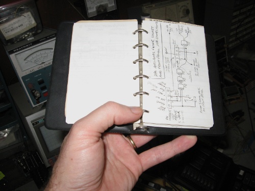 _________________http://WilsonMinesCo.com/ lots of 6502 resources
|
| Mon Jul 28, 2014 1:36 am |
|
|
|
Dr Jefyll
Joined: Tue Jan 15, 2013 5:43 am
Posts: 189
|
mercury0x000d wrote: Anyone see any obvious mistakes I made? Feedback in general is appreciated! Dunno if it's a mistake exactly, but it's certainly an eyebrow-raiser that IC7 (one of your DUARTs) is connected to D15-D8. Usually byte-wide IO devices are connected to D7-D0, regardless of whether/how many other more-significant bits exist. [Edit: my bad; on the 68000 this is perfectly OK.  ] I haven't checked this circuit closely. But I noticed you're using a 74154, which isn't your best choice for a decoder, due to the wide ( .6" ) package, and IIRC it's only available in standard TTL. A couple of 74ACT138 decoders can do the same job better. Do the goals of this project justify inclusion of sixteen RAM ic's? Or were you just having too much fun with the Eagle software... and you got carried away?   cheers, Jeff
Last edited by Dr Jefyll on Mon Jul 28, 2014 3:03 pm, edited 1 time in total.
|
| Mon Jul 28, 2014 5:01 am |
|
|
|
mercury0x000d
Joined: Tue Jun 03, 2014 2:40 pm
Posts: 127
|
Dr Jefyll wrote: Dunno if it's a mistake exactly, but it's certainly an eyebrow-raiser that IC7 (one of your DUARTs) is connected to D15-D8. Usually byte-wide IO devices are connected to D7-D0, regardless of whether/how many other more-significant bits exist. I did intend to do that, but should I not have? I figured I could pack both DUARTs on one address decoder line if they're paired up just like the memory chips. I suppose I could blow another line though since there are so many unused. Would the way they are now be harder to code for? Dr Jefyll wrote: I haven't checked this circuit closely. But I noticed you're using a 74154, which isn't your best choice for a decoder, due to the wide ( .6" ) package, and IIRC it's only available in standard TTL. A couple of 74ACT138 decoders can do the same job better. I ordered the 74154 early on, and since I have it already, I figure I may as well keep it. My logic was, with the EPROMs and SRAM all being 1 MB wide, it's pretty handy to take the remaining 4 lines and use them for steering. To do the same thing with a 3 line decoder like the '138, I'd have to either use two along with a gate to select which decoder to use or just use a single '138 and waste an address line. Since this board is only running at 8 MHz, it's fast enough for now, but the main '060 board will definitely need something faster. Dr Jefyll wrote: Do the goals of this project justify inclusion of sixteen RAM ic's? Or were you just having too much fun with the Eagle software... and you got carried away? ... Um... yes? lol Yeah, I probably don't need a whole 8 megs of RAM in what is essentially a demo board. The only reason I did that in the first place was because once it's done I can start building my BIOS and OS in my spare(  ) time and I have no idea how much memory that will take. I'll most likely reduce it to 4 megs.
Last edited by mercury0x000d on Tue Jul 29, 2014 3:13 pm, edited 3 times in total.
|
| Mon Jul 28, 2014 5:31 am |
|
|
|
mercury0x000d
Joined: Tue Jun 03, 2014 2:40 pm
Posts: 127
|
Garth wrote: It's so big I guess I'll have to wait 'til our son gets the printer in the other room going again. What you can do to make schematics much more compact and legible is use the bus symbol which is like an extra fat wire with the various bus signals coming out at 45-degree angles, as if it were a bundle of wire, wrapped, with individual labeled wires coming out the sides of the wrapping. For an example, see my diagram at http://wilsonminesco.com/6502primer/pot ... ml#BAS_CPUI don't usually draw out a whole computer schematic though. Instead, I have smaller schematics of individual portions-- address decode, reset circuit, interface sections, clock generation, etc., like that in a repair manual for a car, you wouldn't expect to find an exploded view of a headlight assembly in the same diagram with an exploded view of a brake assembly. My workbench computer just has a 3x5" loose-leaf ring binder with 40 pages so far for this computer and another 45 pages for various related projects. I use it frequently for quick-reference. Being pocket-sized, it does not take a lot of workbench space. ... Good ideas! I figured since this is my first board though, I'd draw everything out for my own sanity lol Easier for me to track what's going where. That would be a tremendous space saver though.
|
| Mon Jul 28, 2014 5:32 am |
|
|
|
Garth
Joined: Tue Dec 11, 2012 8:03 am
Posts: 285
Location: California
|
The 74 HC154 is available in 24-lead SOIC, a .300'-wide DIP, and a couple of other packages. http://www.mouser.com/Search/Refine.asp ... rd=74HC154Same for 74HCT154. http://www.mouser.com/Search/Refine.asp ... d=74HCT154Unfortunately, no 74AC or 74ACT or 74ABT, at least not at Mouser. Drawing buses makes it easier to follow idividual lines. They are always labeled where the enter/exit a "bundle" or connect to something. _________________http://WilsonMinesCo.com/ lots of 6502 resources
|
| Mon Jul 28, 2014 7:39 am |
|
|
|
Dr Jefyll
Joined: Tue Jan 15, 2013 5:43 am
Posts: 189
|
Doh! -- sorry. The concern I raised about putting the DUART on D15-D8 was unfounded. What you've done is perfectly OK. (On some processors it would mean the DUART data would appear in D15-D8 of the register, and that would be a nuisance coding-wise.) On the bright side, checking this issue gave me a chance to drag out my decades-old Motorola Microprocessors Data Manual. I'm always glad to have an excuse to go thumbing through that venerable tome.
|
| Mon Jul 28, 2014 2:59 pm |
|
|
Who is online |
Users browsing this forum: No registered users and 16 guests |
|
You cannot post new topics in this forum
You cannot reply to topics in this forum
You cannot edit your posts in this forum
You cannot delete your posts in this forum
You cannot post attachments in this forum
|

|
