Last visit was: Wed Oct 09, 2024 6:18 pm
It is currently Wed Oct 09, 2024 6:18 pm


 [ 4 posts ] 
 Studio 68: an FPGA-centric board for retro "experiments"... 
Author Message
User avatar

Joined: Mon May 04, 2020 3:29 pm
Posts: 9
Hi,
the Studio 68 is a board to make retrocomputing "experiments" with old CPU.
It is an FPGA-centric design so all (or most) of the control logic and I/O can be synthesized inside the FPGA (as a configurable chip set). There is also a STM32 MCU that can be used as "companion processor" (i.e for I/O or boot).
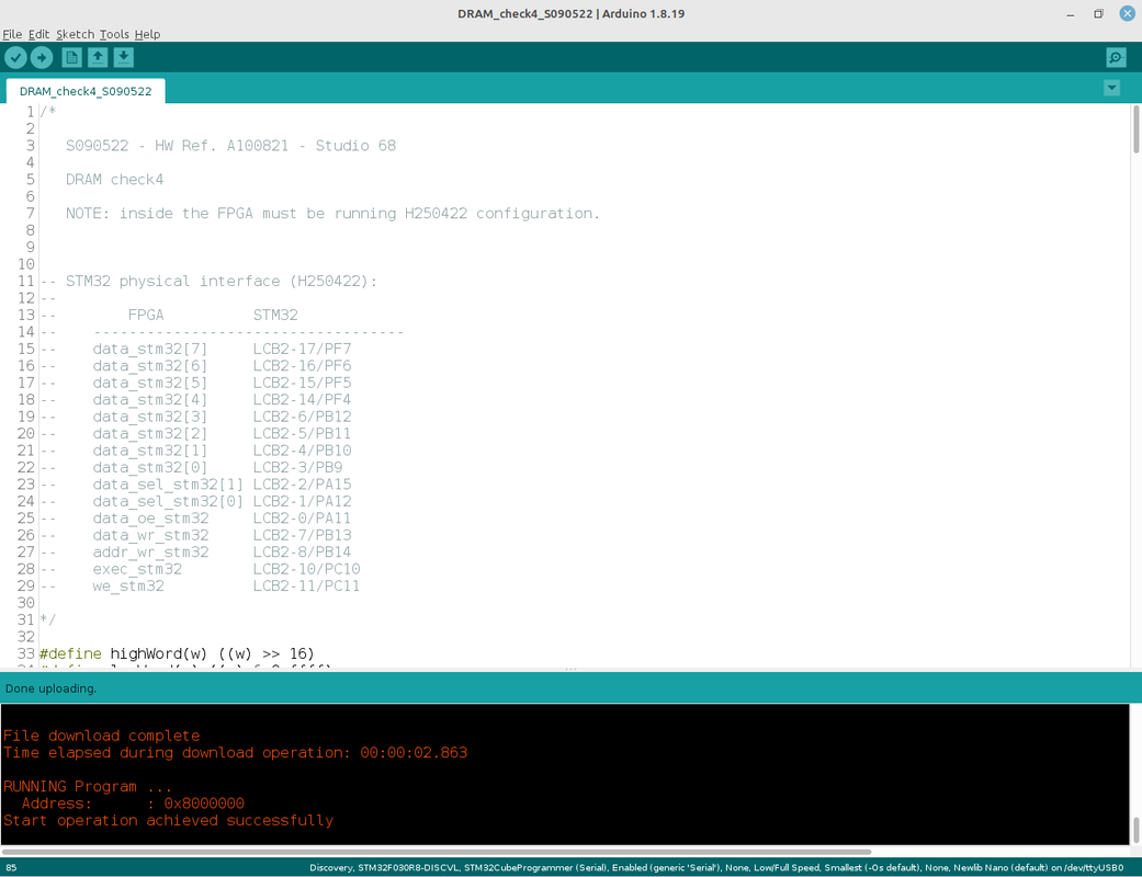
The STM32 can be programmed with the Arduino IDE (with the STM32 "core") as the STM32 section of the board is compatible with the ST Discovery Board with the same MCU.
On board there is also a 68SEC000 CPU just to start playing with it.
More, an external bus with 5V translators allows to add external "Application Boards" with others CPU (putting the internal 68SEC000 CPU in High-Z).
The external bus is completely configurable by the FPGA so it is virtually HW independent.

Here the block diagram:

Attachment:
Studio 68 Blocks.jpg


Here the board (4-layers PCB):

Attachment:
Studio 68_Front.jpg


Attachment:
Studio 68_Back.jpg

Image


and here a first test running the 68SEC000 CPU (all the control and I/O logic is synthesized inside the FPGA, and the STM32 is used as FPGA-serial bridge):

Attachment:
Hello Studio 68.jpg


The next step will be to test the external bus with an "Application Board" with a KR1802VM2 CPU, a Soviet PDP11 clone.
The KR1802VM2 CPU has a fully static design and the clock can be 0Hz, so it can easily connected to a 5V MCU for single clock pulses testing.
So I've done as first step a test board (a "shield" for my development board PicOne) to check some behaviors of this CPU (and of course check if it works :D ) before making the Application Board add-on for the Studio 68, and it's currently on the way...:

Attachment:
A140822.jpg


Attachment:
KR1801VM2.jpg


You do not have the required permissions to view the files attached to this post.


Wed Aug 24, 2022 12:20 pm

Joined: Wed Jan 09, 2013 6:54 pm
Posts: 1799
Wonderful! That's a lot of signals going into and out of the FGPA - very flexible!


Wed Aug 24, 2022 12:26 pm

Joined: Mon Oct 07, 2019 2:41 am
Posts: 649
I have been using DE1, from ALTERA that has a cyclone II on it. How compatable is the your hardware (cyclone ii) with this one?
What do code do you use to access the Dram?
Ben.


Wed Aug 24, 2022 5:20 pm
User avatar

Joined: Mon May 04, 2020 3:29 pm
Posts: 9
oldben wrote:
...How compatible is the your hardware (cyclone ii) with this one?


Hi, I use the same Cyclone II family (and Quartus v13sp1, the last supporting Cyclone II devices) so from the FPGA "point of view" should be 100% compatible. Of course there are differences in the design, and on my board there is also an STM32 MCU.

oldben wrote:
...What do code do you use to access the Dram?


To test the DRAM I've used a VHDL DRAM controller from here with a custom VHDL I/O to drive the DRAM using the local bus connected with the STM32 (accessing the DRAM with it).


Thu Aug 25, 2022 11:31 am
 [ 4 posts ] 

Who is online

Users browsing this forum: AhrefsBot, CCBot and 0 guests


You cannot post new topics in this forum
You cannot reply to topics in this forum
You cannot edit your posts in this forum
You cannot delete your posts in this forum
You cannot post attachments in this forum

Jump to:  
Powered by phpBB® Forum Software © phpBB Group
Designed by ST Software