Last visit was: Tue Sep 10, 2024 9:36 am
It is currently Tue Sep 10, 2024 9:36 am


 [ 108 posts ]  Go to page Previous  1, 2, 3, 4, 5, 6 ... 8  Next
 One Page Computing - roll your own challenge 
Author Message

Joined: Wed Jan 09, 2013 6:54 pm
Posts: 1796
It's great progress indeed Ken, and a very nice board. And an interesting idea to be able to use micropython on the ARM to do assembly.


Fri Aug 25, 2017 3:08 pm

Joined: Wed Jan 09, 2013 6:54 pm
Posts: 1796
Jean-Claude Wippler is writing a blog series "The Fabric of Computing" which, most recently, presents a one-page assembler and one-page emulator for Tim Böscke's "delightfully minimal" CPU which fits in a CPLD:
https://jeelabs.org/2017/11/tfoc---a-minimal-computer/

We've mentioned the MCPU in an earlier thread on Minimal Instruction Set CPUs.


Tue Nov 28, 2017 8:08 pm

Joined: Mon May 28, 2018 8:01 am
Posts: 7
Saw the challenge mentioned on hackaday.io and thought I'd come up with something... and a week or so later here it is:

https://github.com/periata/cpus/tree/master/c61

A 6-bit CPU (designed to be implemented in mostly TTL but using a pair of GAL16V8s for the ALU), with a schematic that fits on a single A4 sheet (at readable size), and ISA description that likewise fits a single sheet of paper (<66 lines, 80 cols).

Features:

* Harvard architecture with 16-bit instruction width * 64 words instruction memory (I suspect there's space to expand that by adding a base register to be shifted and added to the PC ... I would probably expand it out to 1Kword if I had any application that needed that right now -- but I'll leave that for the C61A revision and call this one done for now!)

* two stage pipeline: every instruction writes results back immediately after the next instruction reads its operands. no detection of pipeline hazards, so programmer has to determine which registers are safe to use on each instruction!

* 16 registers in two separate banks (R0-R7, R8-R15) in order to allow two registers to change in a single instruction as long as they are in opposite banks.

* R7 is the program counter (so no jump instruction is necessary: just load a new value into R7 to jump)

* R8 is a data memory offset register, which is shifted left by 4 bits and added to address operands in load and store operations, giving a 1Kword data memory (although my implementation only has 512 words and uses the high address bit to select IO operations)

* R15 is a subroutine link register; whenever R7 is explicitly modified, the old value is copied to R15, thus allowing a simple move to be used to perform call and return operations without needing specific instructions, either.

* Two instruction formats:
1. 3 bits opcode (opcode 7 reserved to select alternative format), 4 bits register A, 3 bits register B (only allows R0-R7), 6 bits immediate word (which is always added to the contents of register B to produce the operand)
2. 4 bits register A, 3 bits register B (R8-R15 only), 6 bits opcode

* ALU designed to be implemented using a pair of 3-bit slices in GAL16V8 chips. Operations: add, subtract, xor, negate.

* Additionally to the standard ALU there are and/or/increment/shift right operations available with optional inverted output (these are type 2 instructions, which end up using a different data path rather than the ALU)

* conditional execution of next instruction: if ra == rb+immediate; if last result was none of selection of (zero, negative, carry); if last result was all of selection of (zero, negative, carry)

* The instruction pointer incrementer can be used to provide a post-increment mode on memory writes (although not reads because that would conflict with access to the register file)

* Designed at gate/standard function block level using "Digital" (a replacement for Logisim that I've found to be a little better for certain things). Other than standard logic gates, components used are: register files (equivalent in behaviour to the 74xx871 IC, only 6-bits wide rather than 4, and only using half of the registers in each of the two chips... I'm sure there's a clever way to multiplex them to avoid the redundancy, but I really can't be bothered), 2-in and 4-in multiplexers, D type latches, adders, comparators (comparing to constants only), delay lines, negater

* Schematic mostly shows direct connections between components, however a handful of signals are connected via "tunnel" components, i.e. the connections are labelled rather than drawn. I think there are less than 5 of these, other than this the connection paths shown are the connections needed.

* RAM needs an access time of cycle time minus propagation delay of a single adder and cycle time less than cpu cycle time (e.g. 90ns SRAM for 10MHz operation)

* Instruction memory needs an access time of half a cycle (e.g. 45ns Flash for 10MHz operation)

Haven't tested the design in hardware, but using 74S* chips for the critical path my estimate is that it should be possible to achieve ~10MHz.
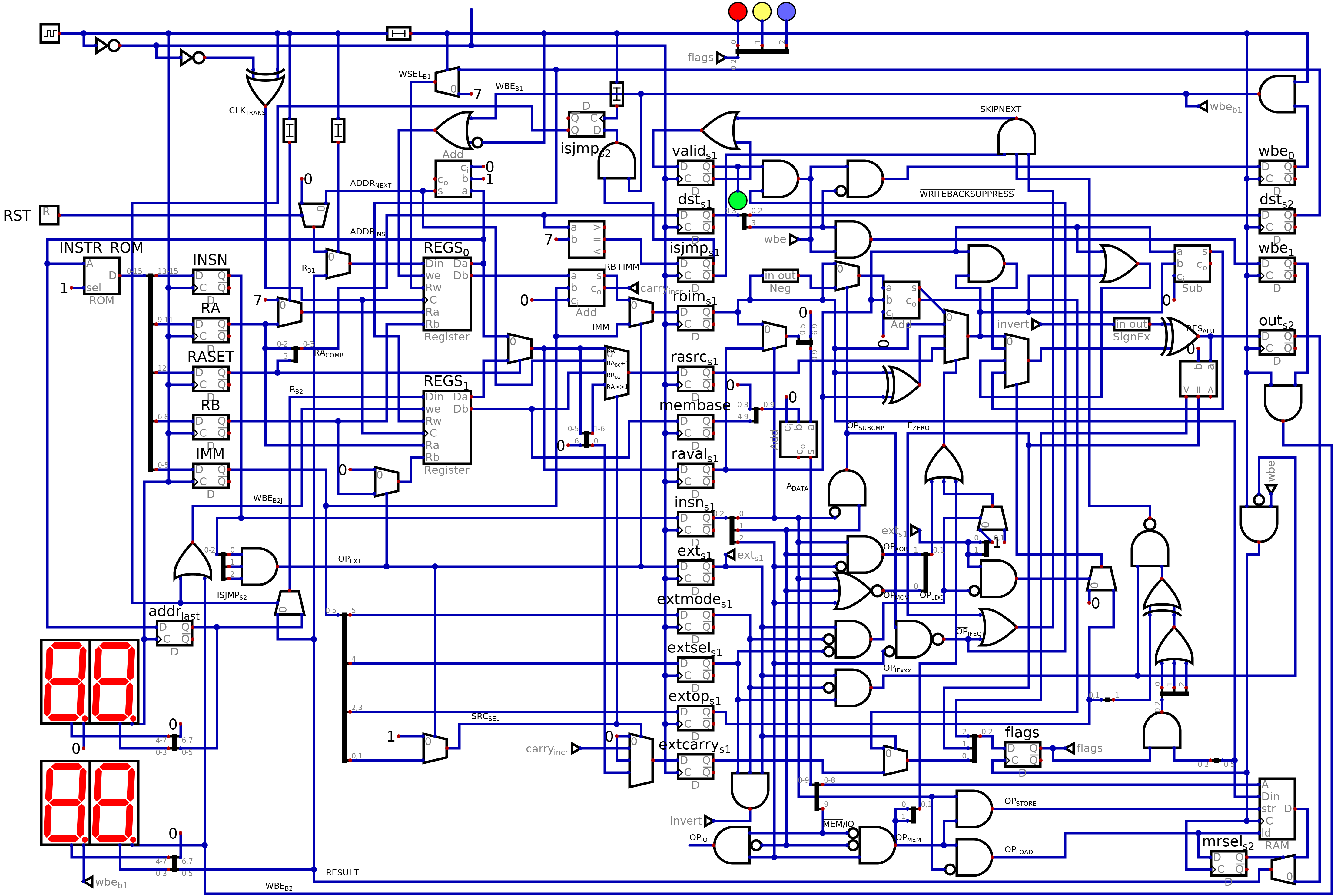
Image


Wed Jun 13, 2018 10:59 pm

Joined: Wed Jan 09, 2013 6:54 pm
Posts: 1796
Interesting - thanks for sharing! Do I take it you have an assembler, or did you hand-assemble?

Harvard should be an interesting simplification though: more busses but each is single purpose.

There must be some 6-bit wide busses, but they are not easy to pick out - do you have any way to highlight them or draw them with a different style?


Thu Jun 14, 2018 10:52 am

Joined: Mon May 28, 2018 8:01 am
Posts: 7
I've hand assembled so far. May hack together an assembler at some point soon, although this project was mostly done as practice for the 12 bit design I'm planning on putting together soon...

Using Harvard architecture definitely simplified things. I originally chose it in order to avoid needing to fetch 3 words per instruction (as 12 bits wasn't quite enough to fit in enough information for the instructions I wanted), but not needing to multiplex the instruction fetch with data memory accesses also made quite a big difference to how I could simplify the structure -- I now have a single memory bus per pipeline stage with no need to coordinate between the two stages.

As to highlighting the buses, unfortunately Digital can't do that. Most of the connections between more complex subcircuits (e.g. latches, adders, etc) are buses. Also note anywhere there's a thick black bar -- those are splitters/combiners for joining buses and individual wires together.


Sat Jun 16, 2018 4:21 pm

Joined: Wed Jan 09, 2013 6:54 pm
Posts: 1796
Ah, I see you've done something about the register ports by splitting into two banks - is that right?


Sat Jun 16, 2018 4:43 pm

Joined: Mon May 28, 2018 8:01 am
Posts: 7
Yes. Two banks of registers so I can write back to two registers simultaneously.

Breaking down the circuit a bit into submodules:

* Along the top edge is clock distribution. I derive three separate clock lines from a standard clock input -- the input as is is used for pipeline stage 1, inverted for stage 2, and I detect transitions (by XORing the two phases) so that the registers (which update on positive edge only) can write back in both phases.

* On the left is the instruction ROM and a set of latches for breaking the incoming instruction into fields, which are latched on positive edge of the clock. The instruction pointer is incremented (through the adder just above the register banks) on the same edge.

* Beneath the register banks is the first stage of instruction decoding: if the opcode is 0x7, then an extended instruction is included instead of the immediate value, and two bits of that instruction are used to select a multiplexer input for the 'a' operand. If the opcode isn't 0x7, the multiplexer input is forced to zero, which selects the register chosen by the 'ra' instruction field. Other choices are: the same register plus one (only available for registers from the top bank) the register from the 'rb' instruction field selected from the bottom bank, or the 'ra' register value shifted right one place.

* At the same time, the 'rb' register value is selected from the top bank and added to the immediate value.

* A comparator connected to the destination register bus detects jump instructions and sets an output flag so they're easier to deal with in the next stage.

* To the right of all this is a bank of latches for the output from stage 1 which trigger on negative edge of the clock.

* Right of the latches at the bottom of the page is the remainder of instruction decoding, extending as far right as the flags latch (the multiplexer above and slightly to the right is decode logic too). This produces signals that drive selecting the correct inputs to the ALU, selecting the ALU mode, determining if the instruction needs to be written back to registers, or if it should cancel the next instruction (which happens if it is a conditional instruction whose condition fails, or if it is a jump).

* To the right of the instruction decode logic is a series of gates oriented vertically: these calculate the outcome of conditional
instructions.

* An adder located adjacent to the 'membase' latch calculates memory addresses (a multiplexer directly above it determines the input).

* RAM access is at the bottom right.

* Above and to the right of the memory address calculator is the ALU.

* The ALU output is fed through a multiplexer (which also takes as input AND and OR functions of the operands, which aren't calculated in the ALU itself, and the result of memory reads) and then through an optional negation before flags are extracted and the result latched for writing back to the appropriate register.

* Above the ALU is logic for determining whether this instruction and the next instruction are to be considered valid, or if writeback is to be disabled for them (easily identifiable by the green LED which is set to show if the current instruction will be written back or not).

* On the right hand edge the results of stage 2 are latched for writing back to the appropriate register.

* Writeback is controlled by logic at the top edge of the page, just to the left of the stage 1-to-2 latches.


Sat Jun 16, 2018 9:24 pm

Joined: Wed Jan 09, 2013 6:54 pm
Posts: 1796
Thanks for the map!


Sat Jun 16, 2018 9:44 pm

Joined: Sat Jun 16, 2018 2:51 am
Posts: 50
This is really neat! Having a blast making my way through the submitted designs.


Fri Sep 14, 2018 8:55 pm

Joined: Sat Jun 16, 2018 2:51 am
Posts: 50
Is a schematic of the OPC available (specifically OPC-6)? Digging through the code, but a schematic would speed things up.


Wed Sep 19, 2018 2:16 am

Joined: Wed Jan 09, 2013 6:54 pm
Posts: 1796
Glad to hear you're interested enough to investigate! No, I'm afraid there isn't a schematic or even a block diagram. Originally the small code size was intended to make the machine almost self-documenting - and there is a logic to the Verilog which follows the idea of a decoder and a datapath - but on the journey from OPC-1 to OPC-6 we did pack in more and more. It might be that you can use that evolution as a sort of training course, building familiarity with the coding style and naming convention starting with the simplest machine. For example, the opc-5 verilog is much more relaxed (as there's less to do.)

As you'll be aware, the spec tells you what it does, but not how it does it:
https://revaldinho.github.io/opc/opc6spec.html

The verilog tells you how it does it, but is not written for readability:
https://github.com/revaldinho/opc/tree/master/opc6

Reading the python emulator in parallel with the HDL might be helpful, although it is again written for compactness.

There is also a C model which is rather more readable, but again it's modelling function rather than structure. Skipping between the three models to build understanding might be worthwhile.

I think possibly starting with the verilog and expanding it with comments might be useful. Especially because the grouping of lines should make some correspondence with structure. Here's my quick take on the verilog:
    lines 1-12: all the interface and internal signals between blocks
    lines 13-19: some signals for initial decode
    lines 20-21: muxes for the outputs
    lines 22-33: decoder
    lines 34-65: control and datapath, with 40-48 being the state machine and 49-63 being datapath


Last edited by BigEd on Wed Sep 19, 2018 9:49 am, edited 1 time in total.

linkify and fix thinko


Wed Sep 19, 2018 7:18 am

Joined: Sat Jun 16, 2018 2:51 am
Posts: 50
Thanks for all the info!
I jumped straight to OPC-6 because it had the most features I wish to learn about. But your advice to start from the first one is a much saner approach. :)


Thu Sep 20, 2018 6:30 am

Joined: Sat Jun 16, 2018 2:51 am
Posts: 50
I'm currently trying to understand how OPC-5 works and a few questions have come up:

1) What does the predicate wire represent?

Code:
wire predicate = IR_q[ PRED_INVERT ] ^ ( ( IR_q[ PRED_C ] | C_q  ) &
                                         ( IR_q[ PRED_Z ] | zero )
                                       );


2) Why use the carry and result registers? Why not just use the C_q and result_q registers?

Code:
reg [15:0] result_q, result;
reg        C_q, carry;

...

always @ ( * )
begin

   // default values?
   result = 16'bx;
   carry  = C_q;
   zero   = ! ( | result_q );

   case ( IR_q[ `i_opcode ] )

      LD  : result            = OR_q;
      ROR : { result, carry } = { carry, OR_q };
      ...

...

always @ ( posedge clk )

   ...

   else if ( FSM_q == EXEC )

      C_q      <= carry;
      result_q <= result;
      ...


3) Why is a separate register PC_q used for the program counter value instead of registerFile[ 15 ]? Ditto for R0. Why is combinatorial logic used to zero the output instead of reading a value of zero from registerFile[0]?

Code:
reg [15:0] PC_q;         // program counter
reg [15:0] GRF_q[15:0];  // register file
reg [3:0]  grf_adr_q;    // register file address

...

wire [15:0] grf_dout;

if ( grf_adr_q == 4'hF )

   // If R15, contents of program counter
   grf_dout = PC_q;

else

   // If R0, zero. Else contents of register
   grf_dout = GRF_q[ grf_adr_q ] & { 16 { ( grf_adr_q != 4'h0 ) } };


Mon Sep 24, 2018 8:52 pm

Joined: Wed Jan 09, 2013 6:54 pm
Posts: 1796
I'll see what I can do. Here's the original code for reference:
https://github.com/revaldinho/opc/blob/ ... /opc5cpu.v

1/ Predication is the idea that every instruction is conditional. So we compute the condition accordingly, and then when it comes time to execute, we choose whether to execute or nop.

2/ I think you're seeing the pipelining here. Or at least, the careful management of clock boundaries. A flop has a D input and a Q output, so the convention in this code is to have 'signalname' be the combinatorially computed value which goes into the flops, and 'signalname_q' or similar as the sequentially delayed value which comes out of the flop.

3/ I think the idea here is to ensure we need only a simple single-ported register file. If PC and R[15] were identical, we'd need two ports (at least for some instruction). For R0, we could either arrange never to write to it, or arrange always to write zero, or arrange never to read it. Looks like the third way was taken.


Tue Sep 25, 2018 8:36 am

Joined: Sat Jun 16, 2018 2:51 am
Posts: 50
With regards to predication, I don't understand how the logic corresponds to this table:

Attachment:
pred.png


When I did a truth table, it seems to be high for seemingly random instructions...


You do not have the required permissions to view the files attached to this post.


Wed Sep 26, 2018 7:47 pm
 [ 108 posts ]  Go to page Previous  1, 2, 3, 4, 5, 6 ... 8  Next

Who is online

Users browsing this forum: CCBot and 0 guests


You cannot post new topics in this forum
You cannot reply to topics in this forum
You cannot edit your posts in this forum
You cannot delete your posts in this forum
You cannot post attachments in this forum

Jump to:  
Powered by phpBB® Forum Software © phpBB Group
Designed by ST Software