View unanswered posts | View active topics It is currently Thu Mar 28, 2024 4:42 pm


Reply to topic  [ 8 posts ] 
 The LD12 - a TTL PDP-8 kit from 1974 
Author Message

Joined: Mon Aug 14, 2017 8:23 am
Posts: 157
Following my interest in the LD20 - mentioned in "The Art of Digital Design"

viewtopic.php?f=3&t=608

After a lot of Googling, I discovered that it had a predecessor known as the LD12.

This was essentially a DIY kit for a functionally equivalent clone of the PDP-8.

Here was a means to build a "workalike" PDP from a kit - but in 1974 it must have been a major undertaking - and costly too.

For some idea of IC costs - the first issue of Byte (Sept 1975) has suppliers ads showing some typical costs of contemporary prices:

https://archive.org/details/byte-magazi ... 9/page/n83

And a 16 pin wirewrap socket was $0.55 - probably adding a further $75 to the build cost.

I have found hand drawn schematics and an assembly manual dating back to 1974.

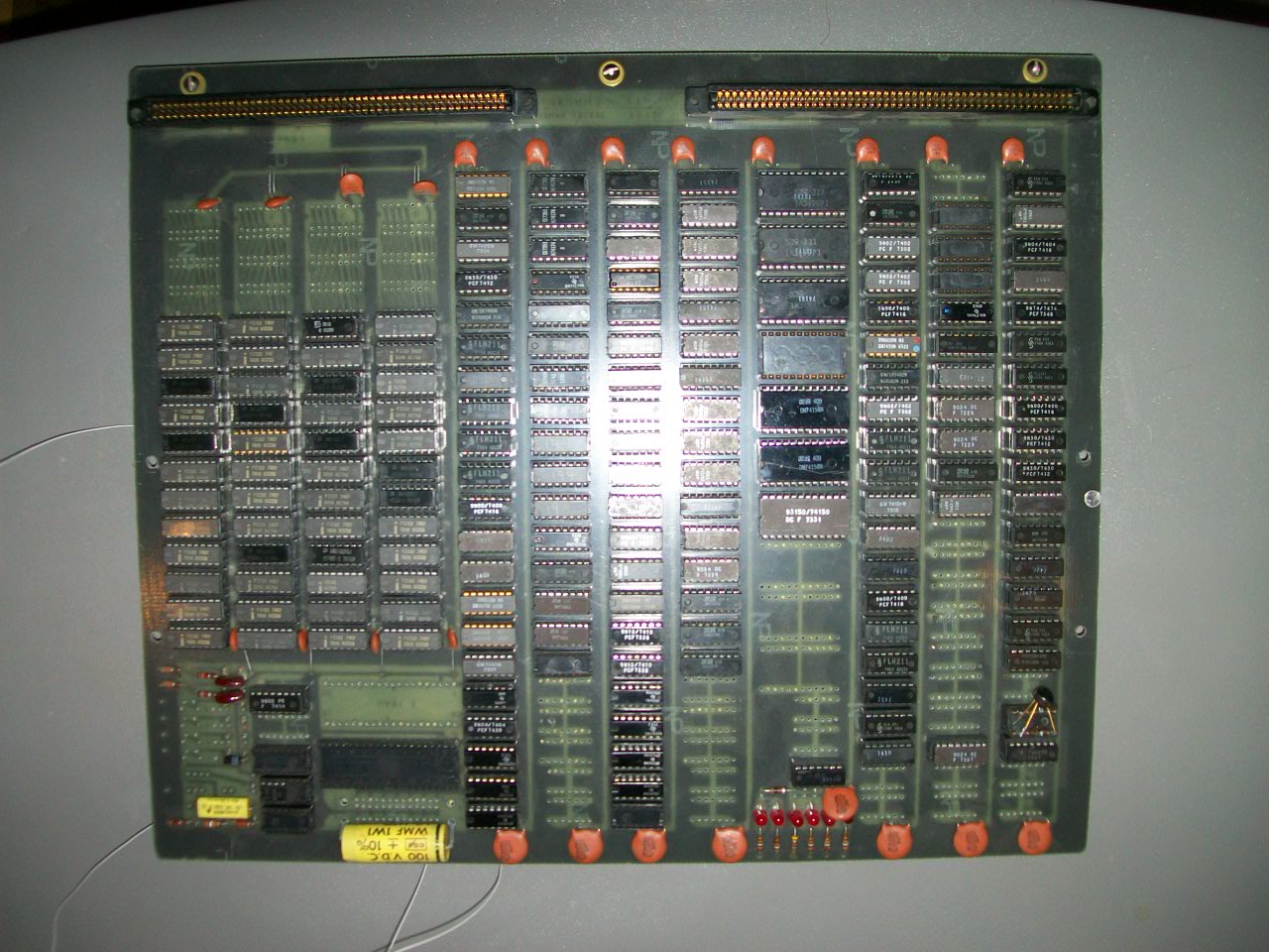
Photographs of the single logic board are here:

https://retrobrewcomputers.org/n8vem-pb ... 0_3908.JPG

The 48 memory chips are on the left - and there is a suggestion, from the 4 empty rows of sockets, and an empty 24 pin socket next to the 74181 ALU section, that there may have been a scheme to extend this design to 16-bit machine.

A link to the schematics and other resource files is here:

https://retrobrewcomputers.org/n8vem-pb ... /96895548/

The basic kit consisted of a large pcb which held in excess of 160 ICs for the 4K machine - with spare sockets for various expansion options such as TTY interface. The pcb tracks provided basic power rail tracks and bussing for the 48 Intel 2102 RAM ICs, but the remainder of the logic had to be wirewrapped!

Pictures of the front and back of this board are in the photos section.

In addition to the logic board, there was a front panel - or Control Panel. This held all the LEDs, switches and the LED driver ICs. The two boards were connected with a pair of connectors - with the control panel sitting horizontally on top of the psu, and the logic board rising vertically at the back.

Semiconductor memory was in the form of Intel 2102 (1024 x 1) up to a maximum of 4K 12-bit words.

It appears from the IC list that memory was not supplied but purchased separately.

IC list shown below

Attachment:
File comment: IC list - not including memory
LD20_ICs.JPG
LD20_ICs.JPG [ 96.14 KiB | Viewed 17810 times ]


Last edited by monsonite on Wed May 29, 2019 5:28 pm, edited 2 times in total.


Wed May 29, 2019 1:32 pm
Profile

Joined: Wed Jan 09, 2013 6:54 pm
Posts: 1780
Great find!


Wed May 29, 2019 3:03 pm
Profile

Joined: Mon Aug 14, 2017 8:23 am
Posts: 157
Hi Ed,

I hope this fills the big gap in the details of the real hardware that was used to support the Prosser and Winkel textbook

viewtopic.php?f=3&t=608

I think that the main logic board was intended to support a variety of minicomputer designs, the PDP-8 being just the first - there is evidence that the memory and ALU could be extended to 16-bit, so they might even been thinking of a 4K Data General Nova.

Another area of the pcb implements the TTY interface - and there is a memory extension from just 16 words implemented in 3 off 7489 (64bit) RAMs to 1k x 12 bit of Intel i2102

There were numerous extra locations for ICs, so once these slots were populated with the relevant ICs, the final architecture was implemented solely in the wirewrap layer on the back. The mother of all prototyping boards!

David Winkel was involved in this hardware from the early beginnings - long before the academic textbook was published some 6 years later in 1980.

I still have some questions - that I am pondering. Why did it take so many chips to implement the architecture?

The basic machine used a lot of ICs - many of these are basic TTL gates. The first question must be why was there so much low-level logic based on simple gates?

Was this part of the part of the educational experience to implement logic equations directly in simple gates?

Back in 1974, were simple gates much cheaper?

Was there no incentive to design for minimum parts count?

Were there specific features of the existing PDP-8I design that influenced the implementation? i.e. copied big chunks of the PDP-8i schematics.

Looking back with some hindsight, I wonder if they realised that the (computer) world was about to change a few months later with the introduction of the Altair 8800. The two machines were designed and developed concurrently during 1974.


Wed May 29, 2019 3:57 pm
Profile
User avatar

Joined: Fri Mar 22, 2019 8:03 am
Posts: 328
Location: Girona-Catalonia
This is all very interesting, and highly informative. Also, in addition to all the questions you posted about design criteria, it’s also kind of surprising to me that the CPU designers of the early times did not realise about the advantages of pure load/store architectures until much later.


Fri May 31, 2019 3:22 pm
Profile

Joined: Mon Aug 14, 2017 8:23 am
Posts: 157
Perhaps it should be remembered that by 1974, the PDP-8 already had 12 years of history, beginning with the LINC and the PDP-5 from 1962/63 which originally defined the architecture and instruction set - based on the early DEC logic modules. The PDP-8 followed on from the PDP-5 in 1965 with improved speed and architecture.

In that period of 12 years or so, the design had changed from DTL to TTL and eventually MSI/LSI. Each design iteration had to maintain software compatibility with the previous generation.

What may have appeared to be a minimal, useful architecture in 1962, which could be implemented economically in DTL in 1962, by 1974 would appear dated and flawed - and was really only perpetuated because of the huge user base of >50,000 machines and the availability of back catalogue software.

If you had started with a clean sheet design for a 12-bit machine in 1974 and not restricted by having to be compatible with the PDP-8 then the IC count may well have been significantly reduced.


Fri May 31, 2019 5:52 pm
Profile

Joined: Mon Oct 07, 2019 2:41 am
Posts: 585
Well have been planning a computer since 74, but the hardware is a tad behind.
For quicker developmrent work ( when the FPGA software compilers working hardware)
I have been using a outdated Altera DE1 fpga development card. With it I can use TTL logic macros
for all my favorite chips. 74181,74670,74157... They would rather push ARM emulation rather than
a 7474 D F/F that they can't emulate. The newer logic cells have only a asyncronus clear, not a preset. The design goal is a 74LSXXX hardware version from about 1975/1976.
This is a 18 bit cpu, using 8 chips for 5 , 4 bit slices in the data path. 2 256x8 and one 32x8 prom
is control logic. CMOS 22V10's will be used rather than real proms. Other than a few minor changes
with 74LS for low power, the basic design is 7400 chip set. The Architecture is Core Memory
with a READ/WRITE back memory cycle. A .750 us state cycle, giving a 1.5 us core memory cycle.
A ballpark number of chips is about 45 for the data path and 30 chips for the control path using MSI
logic. 75 chips in total compared to 110 of the LD12. Of course more chips are neede for I/O, core style memory and the front panel.
A PDP 8 needed only 4 or 8 K of memory ~ 1973. I will need about 32K of memory, 8 K OS, 512 words prom and 24K for software for ~1976 as general purpose computer.


Mon Oct 07, 2019 6:00 am
Profile

Joined: Mon Aug 14, 2017 8:23 am
Posts: 157
Hi Ben,

Thanks for sharing. I'm also working on a design based on 4-bit slices.

I have an Altera Nano DE0 dev-board that I might re-visit, but my preferred FPGAs are the Lattice ICE40 - because of the open-source toolchain.


Mon Oct 07, 2019 2:42 pm
Profile

Joined: Mon Oct 07, 2019 2:41 am
Posts: 585
I got a DE0 nano here too. I put a PDP11 on it from pdp2011 but never got it booted.
My current TTL project is living in the DE1,but I got some software bugs to fix, before I
boot a OS from the SD card. So if you need a 18 bit cpu I have one mostly working.

The biggest problem with the DE1 is that I would get timing bugs with the hardware,
some days it would compile but not run. I seem to have got rid of it by latching control
signals and memory information. The next revsion may be 20 bit rather a 18 bit cpu
so I have opcode space for a deluxe machine like long operations.

Hardware is still the easy part to change, getting software writen for the design is slow,
so If one does build a PDP8, software is around. The only gotya is the disk I/O
must 100% emulate the hardware and be fast, every thing is swapped to and from disk.


Tue Oct 08, 2019 11:55 pm
Profile
Display posts from previous:  Sort by  
Reply to topic   [ 8 posts ] 

Who is online

Users browsing this forum: No registered users and 0 guests


You cannot post new topics in this forum
You cannot reply to topics in this forum
You cannot edit your posts in this forum
You cannot delete your posts in this forum
You cannot post attachments in this forum

Search for:
Jump to:  
cron
Powered by phpBB® Forum Software © phpBB Group
Designed by ST Software